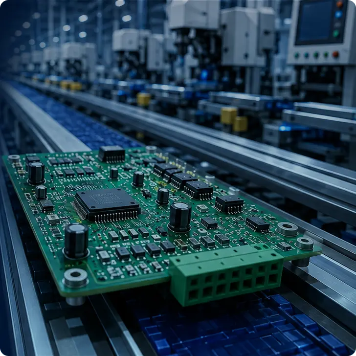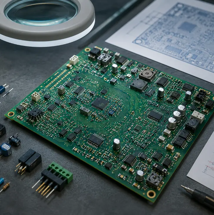
An ageing through-hole design holding a product back.
Through-hole PCB technology was the standard for decades and for good reason. PTH components are robust, easy to inspect, and straightforward to hand-solder. But as a primary assembly technology in a modern production environment, a fully leaded design carries real disadvantages that compound over time.
The client came to us with an existing product built around a through-hole PCB with a 450-component BOM. The design was functional, but it had accumulated the limitations of its era: larger board footprint than necessary, higher assembly time and cost due to the labour intensity of through-hole placement, and components that were increasingly difficult to source as the electronics industry continued its long shift toward surface-mount equivalents.
The objective was clear – convert as much of the design as possible to SMD, replace ageing components with better modern equivalents where the opportunity existed, and deliver a redesigned PCB that was more stable, more cost-effective to produce, and better suited to automated assembly. Without changing what the product did.