Everything You Need to Know About PCB Assembly
 25 Jan 2021
  9 min read
 By jinstpvtltd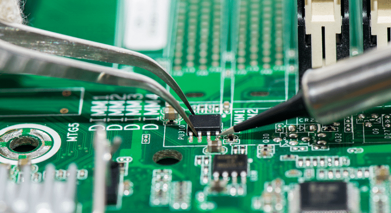
Electronics play an important part in our daily lives. From smartphones to cars, all the devices use electronic components. And the most important part of the electronic device is the Printed Circuit Board (PCB). A common man can easily recognize printed circuit boards in the devices. The PCBs are small green chips layered with copper parts, placed in the heart of the electronic device. Electronic manufacturing services play an important role in designing these PCBs.
The PCB assembly process is the combination of many steps that should be performed in the right sequence and manner to deliver the finished product to function as needed. To make sure this process goes in the right direction, the PCB manufacturers use screen templates and a balanced heating and cooling process to adjust and secure the components into places.
Electronic manufacturing in India works very efficiently by choosing the technology for the components used, aligning the pieces and parts in the right spot as per the needs of the PCB design.
To understand in-depth how exactly the PCB process is conducted, we’ve mentioned in the details below:
- What is PCB Assembly?
- Steps for the PCB Assembly Process
- Areas served by the PCB industries
1. What is PCB Assembly?
Printed circuit board assembly is the process wherein the electronic components are connected with the wires of the PCBs. It is also referred to as PCBA, where the components are soldered to the printed circuit board. There are different methods- manual and automatic used to carry out the PCB Assembly.
Jayshree Instruments Pvt Ltd is one of the best PCB manufacturer company in Ahmedabad.
2. Steps for the PCB Assembly Process
The PCB assembly process steps start with the base, buildup of several layers. Each layer has its importance for the proper functioning of the PCB. The layers of PCB manufacturing include:
- Substrate: To give rigidity to PCB, a base material is used;
- Copper: Layer of copper traces are applied on the functional side; single-sided PCB needs one side application and double-sided PCB requires application on both the sides;
- Solder Mask: A solder mask is applied to the copper later; this is the green color you see in the PCB. This is a necessary step, as the solder mask keeps everything intact;
- Silkscreen: And, a final layer of white silkscreen is applied to the PCB board.
Let’s know the actual PCB assembly process:
Step 1: Solder Paste Application
This is the initial step of the assembly process, that is, to apply a solder paste on the PCB board. A very thin layer of the stainless-steel stencil is layered on the PCB, allowing to apply the paste on the required parts of the PCB. A solder paste evaluations are conducted initially, to know the quality of the solder paste. For evaluation purposes, the solder pastes are selected and the current solder paste is considered as the baseline for comparison.
Step 2: Pick and Place
Once the solder paste is applied to the PCB board, the next process is to move the board to the pick and place machine. Here, surface mount components are placed on the soldered PCB. The pick and place method was a manual one, where humans used to pick the prepared PCB board and placed the SMDs on it. But thanks to the machine world, which is time-consuming and easy-going.
Step 3: Reflow Soldering
To keep the solder paste and surface mount solidified to the board, a process called “reflow” is carried out. After step 2, the board is sent to a conveyor belt; the belt takes the board into a large reflow oven; the temperature of the oven is around 250 degrees Celsius, and the heat of the oven helps to turn the solder into a solder paste.
As the solder melts, the board passes through many cooler heaters, which cooldowns and solidifies the solder paste. And this way the solder mount paste is joined to the PCB.
Step 4: Inspection
So now when the components are soldered, there comes the need for PCB inspection to be done, and we need to check the function of the assembled board. This is necessary because many times, due to some movement in the reflow process, the connection quality might be poor or no connection at all. This can also result in short-circuiting, as the components may get in touch with the other parts of the circuit, which is not preferable.
There are ways to carry out this inspection and correct the errors. These are:
- Manual Inspection: when the batches are small, manual inspection is one of the most effective ways to check the functionality. But as the size of the board increases, it might become difficult to carry out the manual checks process.
- Automatic Optical Inspection: This is one of the considerable methods used for the inspection of the PCB assembly after the reflow process. This is beneficial when the batch size is large and an automatic optical inspection machine is used to carry out the inspection. The machine has a series of high-resolution cameras, reflecting light in a different direction. This light helps to identify the lower-quality solder. This is a faster process and a huge quantity of PCBs can be inspected.
- X-Ray Inspection: This is not a much-used method of inspection and is used for layered or highly complex PCBs. With the help of X-rays, the hidden defaults of the PCBs can be identified.
Step 5: Quality Control
Once the inspection is carried out thoroughly, the next step is PCB quality control. The testing of the board is carried out, to ensure the quality of the PCB connections. The boards with calibration or programming, require many other steps to ensure functionality.
So, step 4 and step 5, are important steps which should be conducted on regular intervals, so that the errors can be fixed and repaired and in turn, saving the time of the PCB manufacturer, materials used, labor and designer.
Step 6: Cleaning
Once the soldering is done on the boards, there are many types of flux or contaminants found on the PCB surface. So it is very important to conduct a PCB cleaning process, this will help in increasing the life lint of the products along with guaranteed reliability.
The benefits of PCB cleaning are:
- Cleaning can help in making the appearance of the PCB board clearer;
- PCB cleaning will also help in eliminating any electrical defect;
- And, also helps in preventive corrosion in the later stage;
There are three different ways of PCB cleaning. These are:
- Manual Cleaning Method
- Ultrasonic Cleaning Method
- Gas-Phase Cleaning Method
Step 7: Functional Test
Once the soldering and cleaning steps of the PCBA are done, the board goes for a final inspection, to test the functionality of the device. This is known as the PCB functional test. During this step, the electrical characteristics of the PCB are tested. The characteristics such as current, signal output, or voltage are tested and any undesirable features are monitored, which determines whether the PCB is passed or failed. The PCB that is unsuccessful, can be recycled again, but that completely depends on the company policies.
So a functional test is the final stage of the PCB Assembly, and as per the results, the device is used.
3. Areas served by the PCB industries
Many sectors are using PCBs; you can come across them in the smallest devices to some huge parts of machines. Below sectors use the PCB applications largely:
3.1 Medical
With the advancement of technology, the health sector has started using PCBs in large numbers. The devices that are used for treatments, diagnostics, and monitoring, all have PCBs.
When it comes to medical PCBs, the reliability and functionality of the device should be perfectly ensured, as with the help of the device diagnosis or treatment of the patient can be done. For implants and all, the PCB manufacturers have to meet the sanitation standards.
The medical devices using PCBs are:
- Pacemakers used for internal purpose have small PCBs;
- CAT, ultrasonic scanners, CT use PCBs, and even the computers that help in analyzing the images;
- Blood pressure, heart rate monitors use electronic components and need perfect readings;
- Insulin, infusion pumps, analgesia pumps help in providing fluids to the sufferer, and PCB helps in the accuracy and reliability of the device;
With the growth of technology, smaller and useful PCBs are possible.
3.2 Military and Defence
Many applications in the military use PCBs, such as vehicles, firearms, communication devices, computers, and others.
Military PCBs should be tough, durable, and reliable as they are majorly used in adverse climates and conditions. Materials like copper and aluminum are used as they can bear the high temperatures and also won’t get oxidized easily. So the PCBs also play a very important role in national security. The defense uses of PCBs are:
- The instruments used to carry out military operations, to monitor the threats and operations of the equipment use PCBs to enable all these functions smoothly;
- Communication devices like the radios and others also use PCB;
- And PCBs are also used in the control systems for equipment like missile detection systems, radar systems and more;
3.3 Consumer Electronics
The usage of consumer electronics is increasing with a pace and each house today has computers, smartphones, laptops and many other electronic household devices. So PCBs play a very important role in our day to day lives.
The PCBs used for the consumer electronic devices need to be small, with advanced facilities, and low cost, so that the final price of the product is comparatively low.
Some of the consumer products using PCBs are:
- Home appliances like microwaves, refrigerators, coffee machines use PCBs;
- Communication devices like radios, tablets, smartphones, and watches majorly use PCBs;
- Televisions, stereos, and video games also use PCBs for smooth functioning;
3.4 Mechanical and Industrial Sector
Industrial and Mechanical sectors widely use the printed circuit board. The PCBs used for these sectors need to be high-powered and durable too. As the usage conditions in the industrial sectors are quite harsh, temperatures are extreme, rough handling and harsh chemicals are used. To fulfill all these factors, thermal resistant materials or durable metals should be used for the PCBs. And to increase durability, thru-hole technology is used.
So though a small green chip, which sometimes might not be noticed also, is a very important part of any electronic device and suitable for many work sectors. Jayshree Instruments Pvt Ltd is one of the major electronic manufacturer companies in Ahmedabad, you can contact us on Contact – Jayshree Instruments Pvt. Ltd